Some rules are meant to be broken.
Unfortunately, none of them apply to PCB design.
Designing and developing printed circuit boards can be an unforgiving process: placing a critical analog line just a few millimeters closer to a noisy clock line might be the difference between a functional widget and an expensive drink coaster. Luckily, many modern software tools provide safeguards to catch critical mistakes before they’re sent out to your favorite PCB fabricator. The most fundamental of these safeguards are the Design Rules.
In the context of PCB design, Design Rules are a set of requirements, restrictions, and constraints that the board must meet in order to be considered a valid design. An example rule might be that the minimum distance between two copper board features (like a trace and the annular ring of a via) must not be closer than 5 mils (5 thousandths of an inch). As the designer places and routes components, Altium will check the board against this rule set. Depending on the user’s preferences, errors can either be reported in the background or prevented in real-time. Sounds great! What’s the catch?
The range of possible applications for a printed circuit board is amazingly broad. As a result, tools like Altium are made to be as flexible as possible. The downside is that there isn’t a single set of design rules that can play nicely with every PCB design. The standard rules that have been developed cover a large chunk of the playing field, but the designer of any reasonably complex board will need to refine these default rules to match the application. Luckily this is a straightforward process in Altium, and we’ve developed some best practices that you can use to get going quickly.
Design Rule Editor
To get an idea of the range of design rules available within the Altium PCB Editor, open an existing design or start a new PCB project. Then, open the PCB Rules and Constraints Editor by clicking Design -> Rules…

The editor window will look like the following:
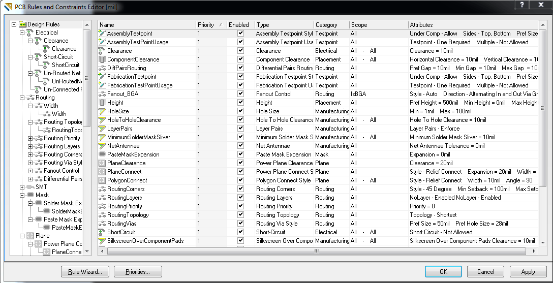
The Design Rules are divided up into several different categories, like Electrical, Routing, Signal Integrity, etc. Expanding a category shows the individual rules that can be modified for each. Let’s go back to the example earlier in this post that defines a minimum separation between copper features. That rule is captured under Electrical -> Clearance. Highlight that rule in the tree view on the left side of the editor to show the details of the constraint.
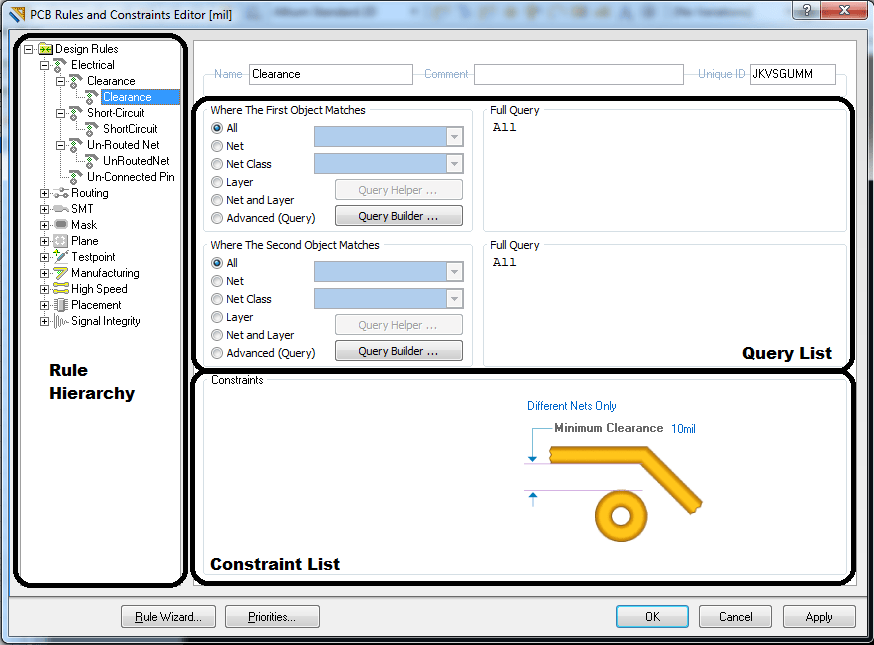
Altium decides how to apply design rules by evaluating one or more queries. In the case of the electrical clearance rule, two queries are executed: one to pick the first copper feature, and the next to pick the second. By default, the query is simply “All” which means that the design rule is applied to every object in the design. For anyone new to the query system in Altium, I recommend reading this article on the Altium Wiki.
The Constraints are then evaluated for each object returned by the queries. Here, any two items that are on different nets (3.3V and Ground, for example) are required to be no less than 10 mils apart. Most of the rules have associated diagrams that illustrate what is being controlled.
Taking Advantage of Rule Priority
There may be situations in your design where two different constraints of the same design rule might apply for different groups of components or traces. An example that has popped up on a few of my past designs applies to the Short Circuit rule (Electrical -> Short-Circuit). In general, short circuits on a PCB are a bad thing. However, I will sometimes create separate nets for my Ground and Shield connections so that I can apply different rules and routing techniques to each. The tie point on the board (where the shield and ground meet) will usually be a copper region to which both nets will connect.
The default Short-Circuit rule will prevent me from making this connection (or at least give me a warning… more on this distinction later). However, I can modify my design rules so that this connection is allowed by manipulating the rule priority.

Notice in my rule hierarchy that there are now two short circuit rules, listed in descending priority:
1. ShortCircuit_GroundShield
2. ShortCircuit_Default
When there are multiple rules defined for a rule category, Altium applies a priority ranking system to decide which rule will be executed. First, the query (or queries) for each rule is evaluated. If multiple rules apply to a set of query results, the highest-priority rule will be executed.
In this example, the ShortCircuit_GroundShield rule applies to objects where the first is in the net “GND” and the second object is in the net “SHIELD”. The ShortCircuit_Default rule applies to any two objects. Clearly, there is some overlap in the scope of these rules. If my board had three nets – 3.3V, GND, and SHIELD, no short circuits would be allowed between 3.3V and GND or 3.3V and SHIELD, but would be allowed between GND and SHIELD.
Editing rule priority can also be useful if a small number of components have requirements that differ from the majority of the board. For example if the minimum trace spacing for the board is 5mils, but a noisy net needs to be 10mils from any other, a new clearance rule (with a higher priority than the default rule) can be added that applies only to the noisy net.
Automating Rule Creation
Altium has a built-in tool called the Design Rules Wizard that provides a friendlier interface for adding design rules to the project. I haven’t used it often (I prefer the query system, which is immensely powerful), but I do know that it is very quick to add a new rule without needing to dig far into the Rule Editor window. You can access this tool in Design -> Rule Wizard…
Importing and Exporting Design Rules
“But Ryan, I’m a rebel and can’t be trusted creating rules! What can I do?”
Despite my thoughts on the matter, I understand that some engineers are just edgy by nature. It’s okay, you’re covered. Design rules can be imported and exported within Altium, so you’re free to use rules from a more responsible source. To import or export design rules, first open the PCB Rules and Constraints editor, then right click on any item in the rule hierarchy. Select either “Import Rules…” or “Export Rules…” If you’re exporting, you can pick which rules will be included in the output file by selecting the relevant items.
A handy tip: if you know what manufacturer will be fabricating your design, see if they have design rules available that match their capabilities. Sunstone Circuits (an Oregon-based PCB manufacturer) has a compatible set of design rules for Altium available on their Downloads page.
Design Rule Check
“Okay, my design rules are set up. Now what?”
At any time, you can check your design against the current rule set by clicking Tools -> Design Rule Check… This will open the Design Rule Checker, which allows you to select which rules will be enabled, as well as how the results will be reported.
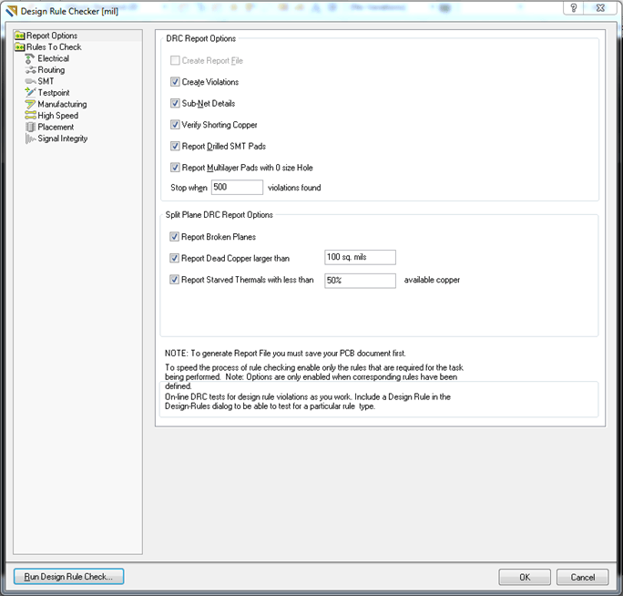
Clicking “Run Design Rule Check” will perform the DRC, and will display the results in an HTML report (this is also saved to the project directory for access later). An example report might look like the following:
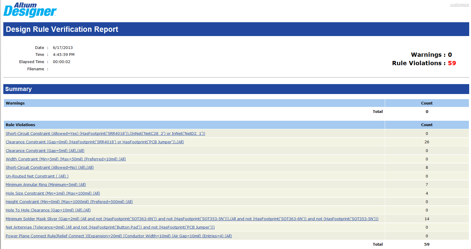
Each of these violations are linked to the coordinates on the PCB that they were observed (clicking on the violation will take you there), which makes it easy to identify the cause and (hopefully) the remedy.
Online DRC
Seeing the mistakes you’ve made is one thing, but it’s more efficient to avoid mistakes instead of going back to fix them. Altium has a feature called the Online DRC that will prevent you from making mistakes in real-time, or at least warn you if you’re violating a rule. Enable this functionality in the Preferences window (Tools -> Preferences…), under the PCB Editor -> General -> Online DRC.
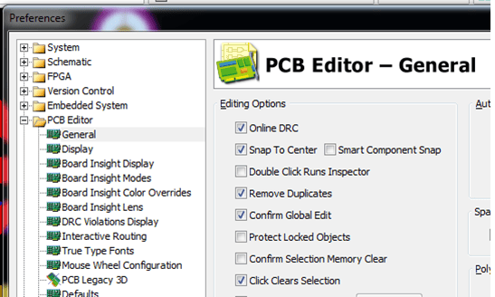
The default settings for the DRC are acceptable for most designs, but you can change which violations are checked and how they are displayed in real-time by navigating to the DRC Violations Display tab within the preferences window.
Final Thoughts
Congratulations, your safety net is now installed! Altium’s Design Rule functionality is one of the most powerful and important features of the PCB editor, and I recommend that careful attention is paid to setting them up before the design is started. Nothing is more frustrating than getting halfway through a design and then realizing that a critical requirement has been blatantly violated all over the place.
No safety net is perfect and you should always take steps to verify your design beyond the design rule check (whether that is a peer review or a prototype run). That said, I hope you found this tutorial informative and useful. Leave any comments or questions below and don’t forget to check out the other articles in the Exploring Altium series!
Pin Swapping
Document Management