Since joining the DMC team, I’ve had the opportunity to contribute to a wide variety of awesome projects and learn several new technologies. During a recent embedded design project, I was tasked with converting our circuit schematic to a printed circuit board (PCB) layout using a software package called Altium Designer. Altium is a very powerful tool for schematic capture and layout (as well as FPGA design and simulation) with a fantastic support wiki, and I wanted to share some of the tips I’ve learned to help anyone involved in the PCB design process.
Pin Swapping
Microcontroller- and FPGA-based designs with a significant number of I/O connections can be challenging to route, particularly on two-layer boards or in compact form factors. Luckily, Altium provides a powerful method of simplifying the layout process on-the-fly: pin swapping.
Consider a simple system where a microcontroller interfaces over a two-wire bus to an LCD driver that updates forty individual segments. Even with an LCD segment multiplexing scheme (a common feature of dedicated LCD driver chips), there are many connections to be made between the driver and the LCD. Making these connections becomes an even bigger challenge as the board size shrinks or additional functionality is added to the system.
Since the pin mapping between the driver and LCD is determined by the microcontroller’s firmware, the physical pinout between the devices are, in essence, arbitrary as long as every segment on the LCD is connected to a pin on the driver. This property, which is common in designs with many I/O, allows the engineer to change the pinout of a device if the current scheme is difficult to route.
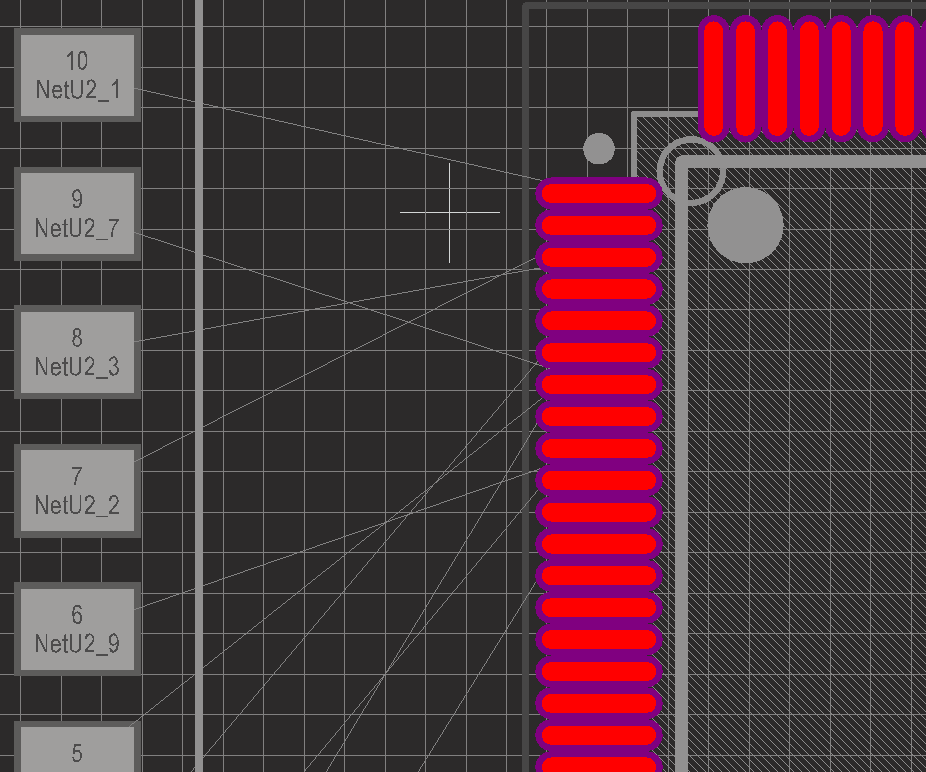
Let’s look at a simple example design with a 10-segment LCD:
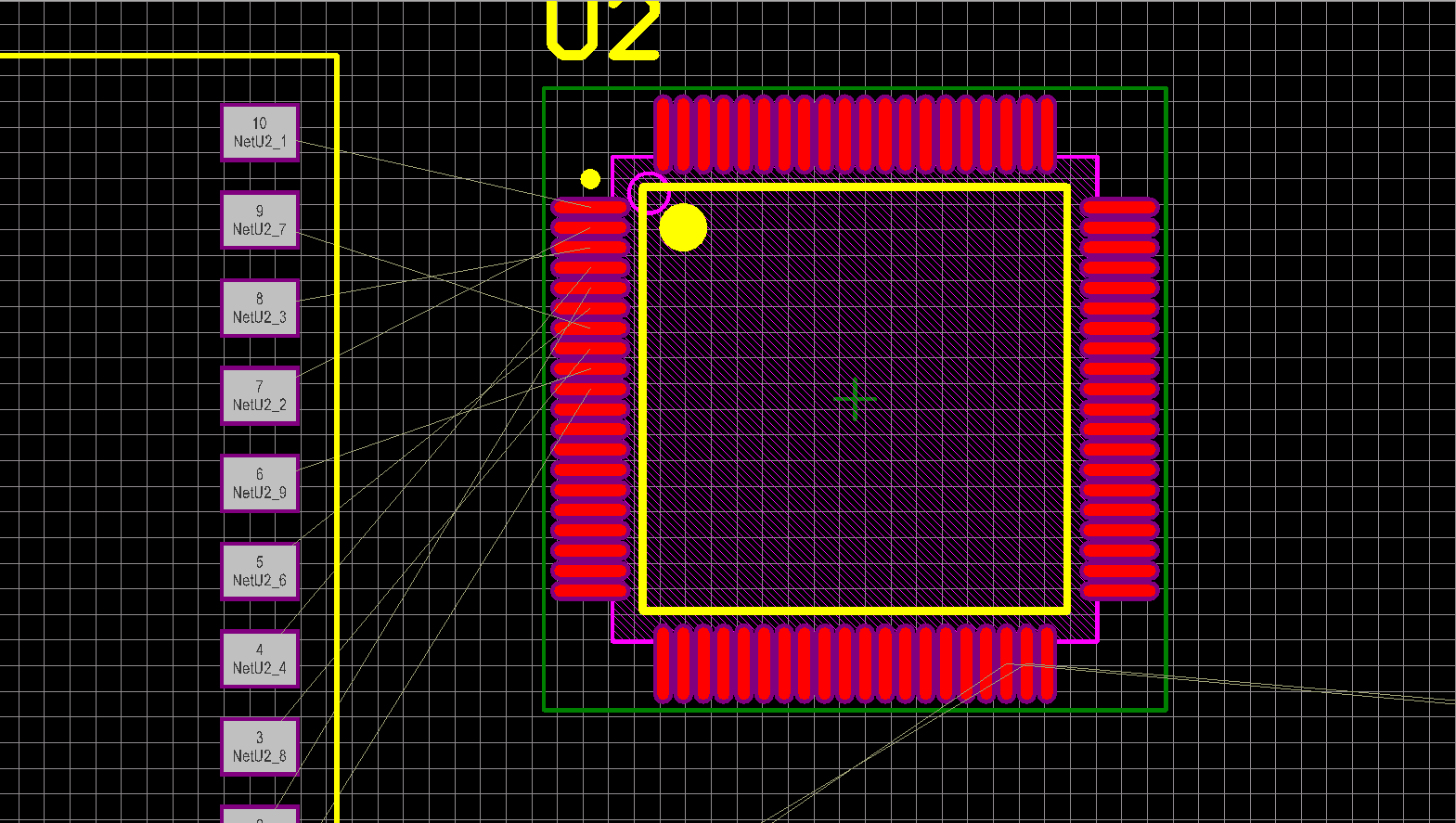
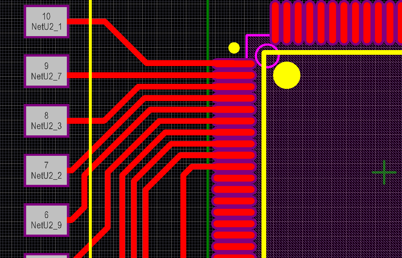
With the current connection scheme, several pins must cross in order to complete the routing. Clearly, it would be much simpler to change the pin mapping to avoid the need to cross the signals. One solution to this problem is to change the connections on the schematic, create an Engineering Change Order (ECO), and push the modification to the layout. Unfortunately, this is a time consuming method that may need to be performed frequently during routing.
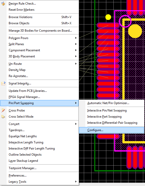
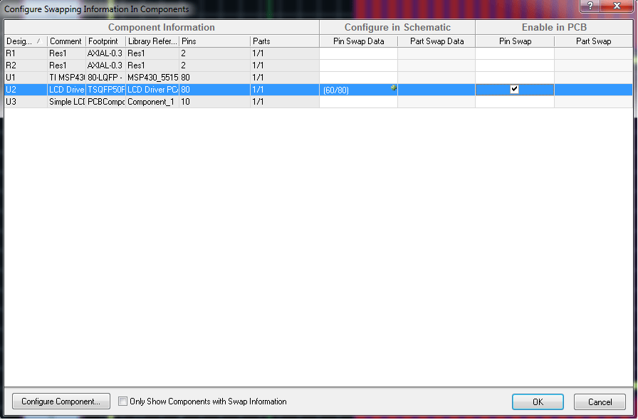
In Altium, however, pin swapping can be employed to automate this process. With a PCB layout document opened, select Tools-> Pin/Part Swapping -> Configure… (keyboard shortcut: T, W, C) to open the pin swapping configuration menu. This dialog lists all of the components in the design and summarizes the current swapping configuration for each device.
Pressing Configure… in this dialog box will bring up the pin swapping menu:
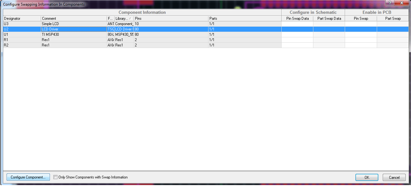
In this example, the LCD driver pins can be re-mapped freely, but the power, ground, and communication pins must stay the same. Selecting this chip and clicking Configure Component… will display a dialog box similar to the figure below:
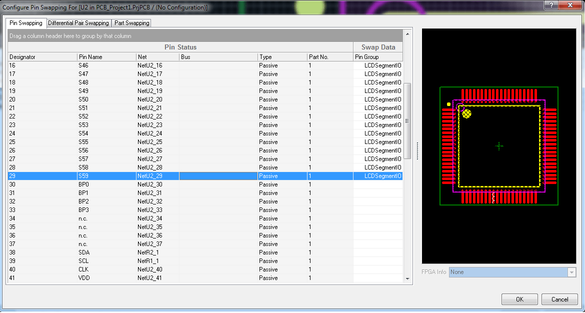
Under the Swap Data section, there is a column titled Pin Group. In these fields, the user can create subclasses of pins that are freely interchangeable. For the LCD driver shown, there are 60 pins that can be mapped to any LCD segment. This group will be named “LCDSegmentIO.” All other fields will be left blank, which prevents them from being swapped.
Note that you can create any number of pin subclasses during this step. For example, if a microcontroller design used one port’s input interrupt functionality for monitoring critical signals and the rest of the ports for general I/O, these could be divided into separate subclasses (say MicroGeneral_IO and MicroInterrupt_IO). In this case, pins mapped to the interrupt-capable port can be swapped with each other, but not with general I/O pins.
To enable pin swapping for the device, press “OK” to return to the Pin/Part Swapping Configuration dialog, and click the checkbox next to the component in the Pin Swap column (under the Enabled in PCB heading). Press “OK” to return to the PCB layout.
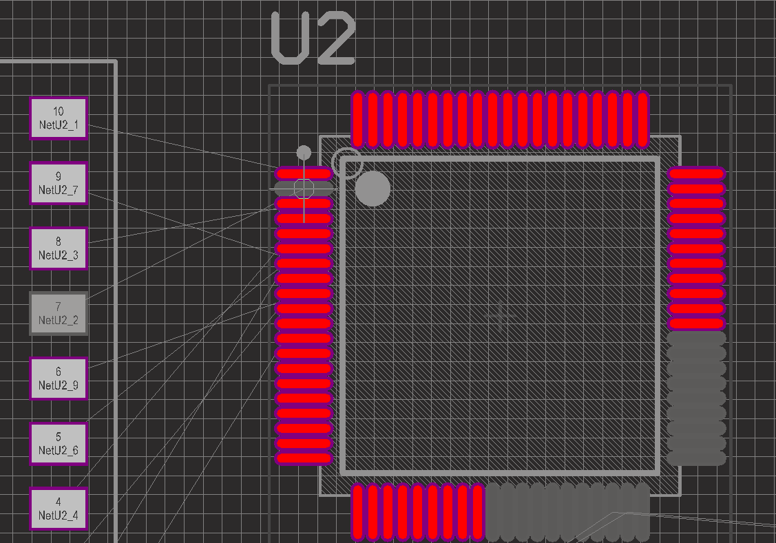
With the preparation work complete, it’s time to simplify the routing between the driver chip and LCD. Save the project, then enter pin swap mode by clicking Tools -> Pin/Part Swapping -> Interactive Pin/Net Swapping (keyboard shortcut: T, W, I). The cursor will change to a crosshair and pin swap-enabled pads will be highlighted. (If the display does not change, ensure that you have enabled the component. Also, pin swapping can only be performed on unrouted nets).
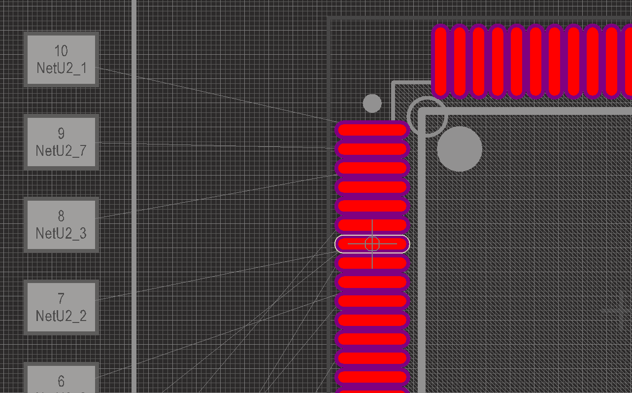
In this case, we will swap the connections for pins 9 and 7 of the LCD to uncross some of the nets. The order of selecting the two pins is unimportant. Clicking on pin two of the LCD driver (which is currently mapped to LCD segment 7) begins the pin swap:
After choosing the first pin, Altium will mask everything except for eligible pins in the same subclass that can be swapped (and anything connected to their respective nets). Pin five (which is mapped to segment 9 of the LCD) is in the correct subclass, so we will choose that as the swap target. Clicking on that pin performs the swap and returns the user to the interactive pin swapping menu.
Much better! Let’s go ahead and pin-swap the remaining nets, and then route all of the traces.
So easy, even an auto-router could do it.
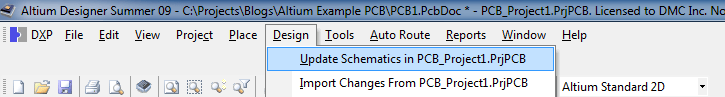
One final step is required before the swap is fully complete: the schematic must be updated to reflect the change. This can be performed after all pin swapping on the PCB is complete. Click Design -> Update Schematics in [Project Name] to create an ECO. The pins on the schematic symbol will be renamed and renumbered to reflect the change.
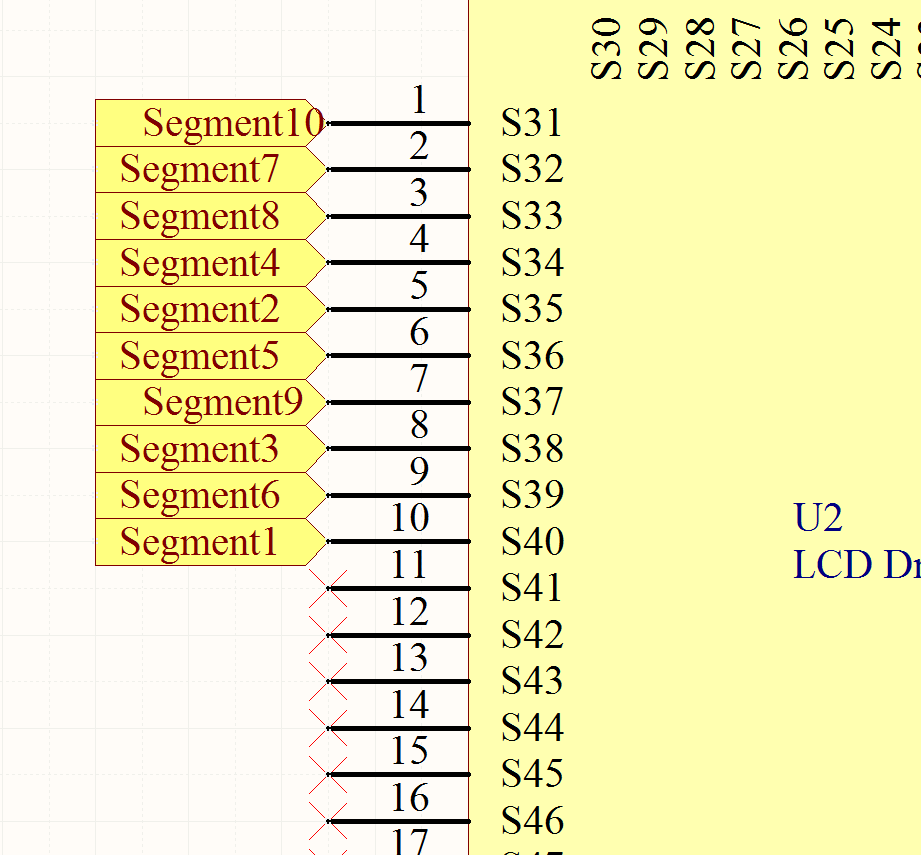
Here is our LCD driver schematic before the back-annotation:
And here it is again afterwards:
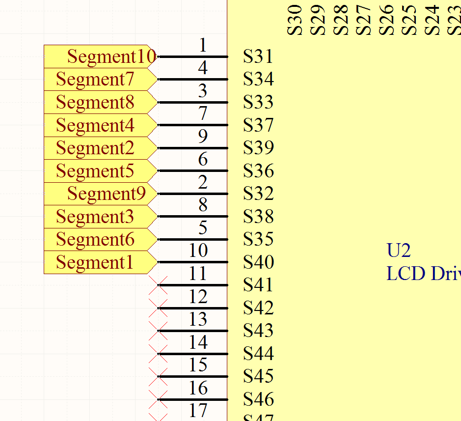
Having used this technique many times on a few different PCBs, I’ve noticed one downside to pin swapping. When you back-annotate a large number of changes to the schematic, the ordering of pins on the schematic symbol tends to deviate wildly from the default numerical order. Trying to look for Pin 56 on a pin-swapped microcontroller can grow from a quick glance to a 15-second search. That said, considering the time saved during the routing process, this is a very minor setback.
Overall, this is an incredibly helpful technique that can be exploited to simplify complex PCB routines significantly. You can learn more about advanced applications of pin swapping in Altium on their support website. Stay tuned to the DMC blog for some upcoming Altium-related posts!