Engineers at DMC often tend to have fun tech hobbies to work on in their spare time. I worked on such a project a couple years ago and wanted to share it on our blog. I came across this webpage while looking for cool LCD projects: Connect Nokia LCD to LPT port
This particular person had connected a Nokia 3310 LCD to a computer’s parallel port and written a PASCAL program to draw on the LCD screen using his mouse. Upon reading this I thought - why not do this with a microcontroller instead of a computer? Wouldn’t it be a lot more fun to interface a PS/2 mouse and this LCD to a microcontroller instead? Since I’m a huge fan of assembly language, I decided to write the code in assembly language which is a lot of fun (though admittedly a little time consuming).
Hardware/Software
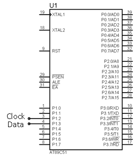
- AT89C51 (8-bit 8051 microcontroller)
- Nokia 3310 LCD(which includes pcd8544 controller)
- PS/2 connector
- RS232 connector(for sending packets received from the mouse to a computer, only for debugging)
- Max-232(for TTL-RS232 conversion)
- HM-6116 (2K SRAM)
- 74LS10(3 input NAND gates)
- 74LS02(2 input NOR gates)
- Stripboard
- Proteus for circuit design and simulation
Mouse-Controller Interface My first task was to interface a PS/2 mouse with the 8051 microcontroller and establish communication. I found this helpful tutorial on the web that explains PS/2 protocol and shows communication packets between a PS/2 mouse and Win98: PS/2 Mouse Protocol
The pinout for a PS/2 port is as follows: 6-pin Mini-DIN (PS/2): 
1 - Data
2 - Not Implemented
3 - Ground
4 - Vcc (+5V)
5 - Clock
6 - Not Implemented
I connected the clock line to pin 2 and data line to pin 3 of port 1 which is a bi-directional IO port.
Mouse-Controller Communication
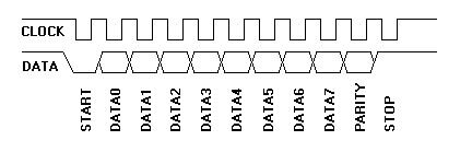
Only Data and Clock pins of the mouse connector are used for communication. The mouse drives the clock. The microcontroller can inhibit communication anytime by pulling clock low. The microcontroller can send commands to the mouse by first sending request to send. It initializes the mouse this way, sets sampling rate, select different modes etc. For sending a command, I send a low on data and a high on clock for a request to send and then poll the clock line until the mouse makes it high so I can send the start bit of the command byte.
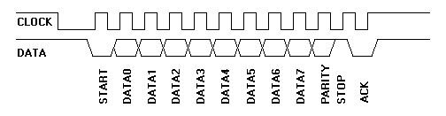
By sending 0xF6 ‘set defaults’ command the mouse goes into stream mode in which the mouse sends a data packet whenever there is movement or if a button is pressed or released. The microcontroller releases the data and clock lines and waits for the mouse to pull the clock low and then reads the start bit. The mouse drives the clock and the subsequent bits are read in a similar manner.
|
Data
|
Clock
|
Bus State
|
|
High
|
High
|
Idle
|
|
High
|
Low
|
Communication inhibited
|
|
Low
|
High
|
Controller: Request to Send
|
LCD-Controller Interface 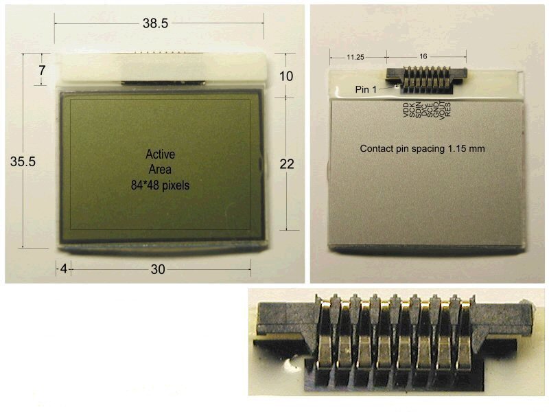
My next task was to get my hands on a Nokia 3310 LCD. I went to a cell phone repair shop and got it just for 100 rupees (1 USD). I soldered fine copper wires to the terminals of the LCD and connected (SCE, SCLK, RES and D/C) to pins of port 1 and 3 as shown in the main schematic below at the end.
|
SCE
|
Active low enable pin
|
|
SCLK
|
Clock signal
|
|
RES
|
Active low reset to initialize chip
|
|
D/C
|
Mode selector 0 for command, 1 for data
|
LCD-Controller Communication
The microcontroller initializes the LCD and sets bias values, temperature coefficient and voltages by sending the proper commands to the pcd8544.
A byte is sent serially to the SDIN input pin. The D/C pin controls whether it is a command or a data byte. After reset and proper initialization, the address is selected by sending command bytes and data bytes are sent to show the corresponding pixels. For more information on commands, read the datasheet of the LCD controller.
The minimum time required for SDIN to maintain its level after the SCLK goes high is 100ns which is much less than the machine cycle. I used a 12 MHz oscillator to drive the 8051 and one machine cycle of the 8051 was calculated to be 1 µs. So there wasn’t any need for timer delays.
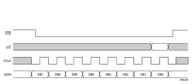
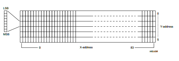
When you initialize the LCD controller and select vertical addressing using a command, its internal RAM address X and Y will be set to 0. When you send it a data byte, it writes the byte to the screen. So if you send a 0x07(00000111), the 6th, 7th and 8th pixel counting from top left to bottom on the screen will be lit. And the X address will automatically be incremented by 1. Note that this is a 48 x 84 pixel LCD so the address ranges for X and Y are 0 to 83 and 0 to 5 respectively. Below is an image that shows addresses of LCD controller’s internal RAM. For more information, please refer to the datasheet.
I scaled the movement of mouse in the horizontal and vertical direction to change the X and Y address of the LCD. When the user presses the left-click button, a data byte is sent in which only one bit is high based on the location of the “cursor” on the screen and the corresponding pixel gets lit. When I got to this point, I noticed that all of the other pixels in that column(byte) got erased. This was a problem because I couldn’t draw anything on the LCD without erasing the previously lit pixels in the same byte and I realized I needed some external RAM to store the already lit pixels and then set only the bit where the cursor is present and mask the other 7 bits. The internal RAM of the 8051 was 128 x 8-bit which wasn’t enough to store 48 x 84 = 2520 pixels. So I used a HM-6116 (2K SRAM) because it was easily available to me. To display images on the LCD screen like the one shown in the image of Proteus simulation below, I used a tool called FastLCD to make hex files for those images. For writing characters to the screen, I used the font hex files from JAL Library.
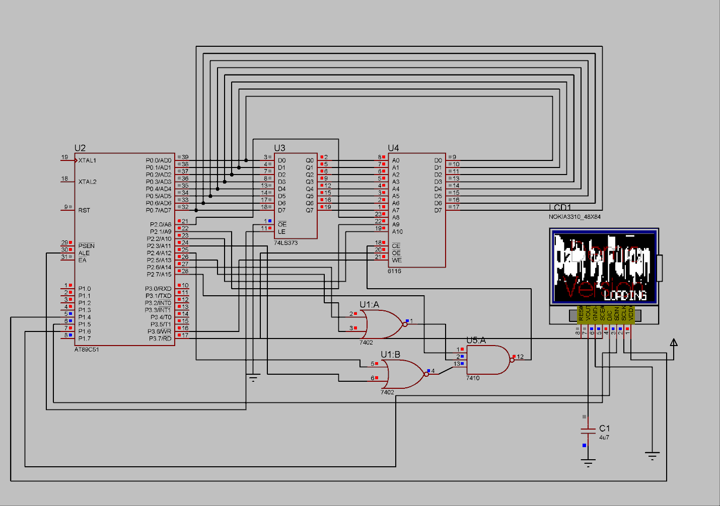
Note that there is no mouse in this schematic because I couldn’t find a mouse model in Proteus for simulation.
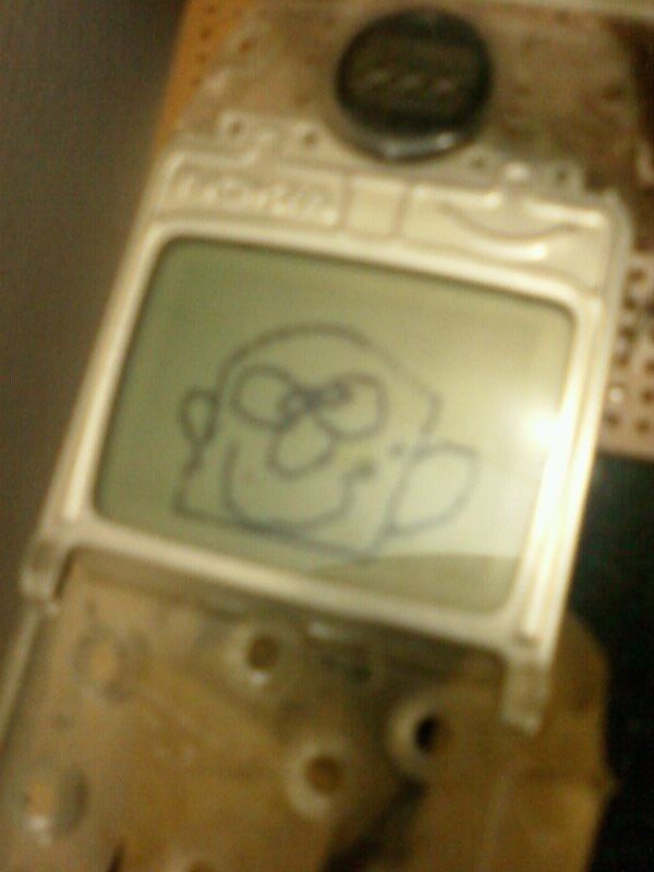
Something I drew on the screen using my mouse.