One of my absolute favorite things about embedded design is watching a product evolve over the development cycle. From unboxing the first prototype all the way to the release of the deluxe commercial model, each revision of the design poses new and interesting challenges. One of these challenges is managing each revision of the electrical schematic and PCB layout in a way that minimizes human error and maximizes automation.
Altium Designer has an excellent tool to assist the embedded engineer in managing changes between revisions and within different variations of a base design: Design Variants (sometimes called Assembly Variants).
Introduction to Design Variants
So, when do Design Variants come into play? At DMC, we use this tool primarily to manage situations where components that exist on the schematic are not intended to be installed on the PCB. There are many reasons why a component might be placed on the schematic but not on the final board. Here are a few key cases:
- Designs with functionality that can be stripped away for "basic" flavors of the product/solution
- Prototypes intended to test functionality of two or more similar (but not identical) circuits; one example would be evaluating two 5V power supplies for the lowest noise
- Designs with a matrix of pull-up and pull-down resistors to indicate the PCB/hardware revision to the microprocessor so that it can re-assign I/O addresses or enable/disable functionality accordingly
Let's take the first case above. DMC recently executed an embedded design for Chicago Dial Indicator (CDI), a company that manufactures (among many other products) high-quality electronic dial indicators. DMC originally connected with CDI to help innovate their flagship electronic dial indicator (you can read more about that project here). After launching that product, CDI approached us again to revitalize their EMS device, which connects multiple indicators to a single device to show data, log measurements, and provide an easy interface to a PC or measurement system.
DMC suggested designing a PCB that could interface with an expansion board to double the channel count without any additional hardware designs. Sure, we could have designed and managed two separate boards, but with Altium's Design Variants functionality, this was a breeze. Let's take a look!
Variant Management
Below is an excerpt of the schematic that shows the device interface channels. Rather than copy-pasting each individual channel, we're using the multi-channel functionality of Altium, which you can see above the sheet symbol for a device channel: REPEAT(MTI,1,4) will create four copies of the sheet, MTIA, MTIB, MTIB, and MTIC

In the upper-right hand corner (by default) of the schematic editor, you'll find the Design Variants button, which launches the Assembly Variants Management window.
Adding a New Variant
Launching the Variant Management window will show you a screen like the following:
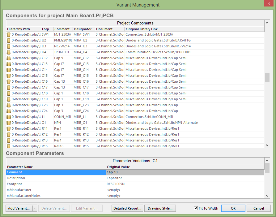
For the Basic version of this PCB, we only want to populate two of the four channels (MTIA and MTIB). First, let's add an assembly variant called "Basic". Find the "Add Variant..." button on the bottom left of this window and click it. You will see the "Edit Design Variant" window below:
I selected "Allow variation of fabrication outputs." This isn't critical, but sometimes you'll want to omit certain footprints for components that are not installed.
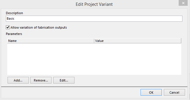
After clicking OK, you should see the Variant Management window again with a new column for the variant you created. Let's find the components that will not be fitted for the "Basic" variant of this design. In my case, I am de-populating channels MTIC and MTID, so I'll highlight any components with either of those prefixes in the "Designator" field.
To bulk-edit these parts, right-click on the highlighted "Component Variation" field, hover over "Set Selected As" and then click "Not Fitted".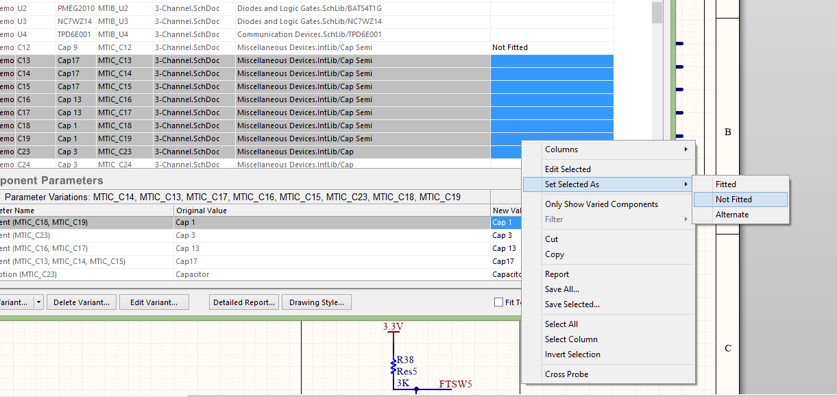
After this action, all of the highlighted parts should now show "Not Fitted" in the Component Variation field.
Design Variants and the Schematic
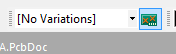
Now that your design variant has been created and configured, it's time to take a look at the schematic to check our work. Find the Design Variants button again (in the upper-right hand corner of the schematic editor by default). Next to it is a drop-down menu that shows the selected Design Variant. This field will probably show "[No Variations]." Click on the drop-down and find the variant you just created.
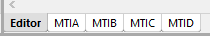
The default view of the Schematic Editor is the "Editor" view (so creative). If you look on the bottom toolbar, however, you will see one or more tabs next to "Editor." In the case of multi-channel schematics, each of the individual channels will be accessible here. If the schematic is only used once, there will only be a single tab.
If I click on channels MTIC or MTID, the two channels that will not be installed on my Basic variant, the schematic editor will show red x-marks over all of the components that are marked as Not Fitted.
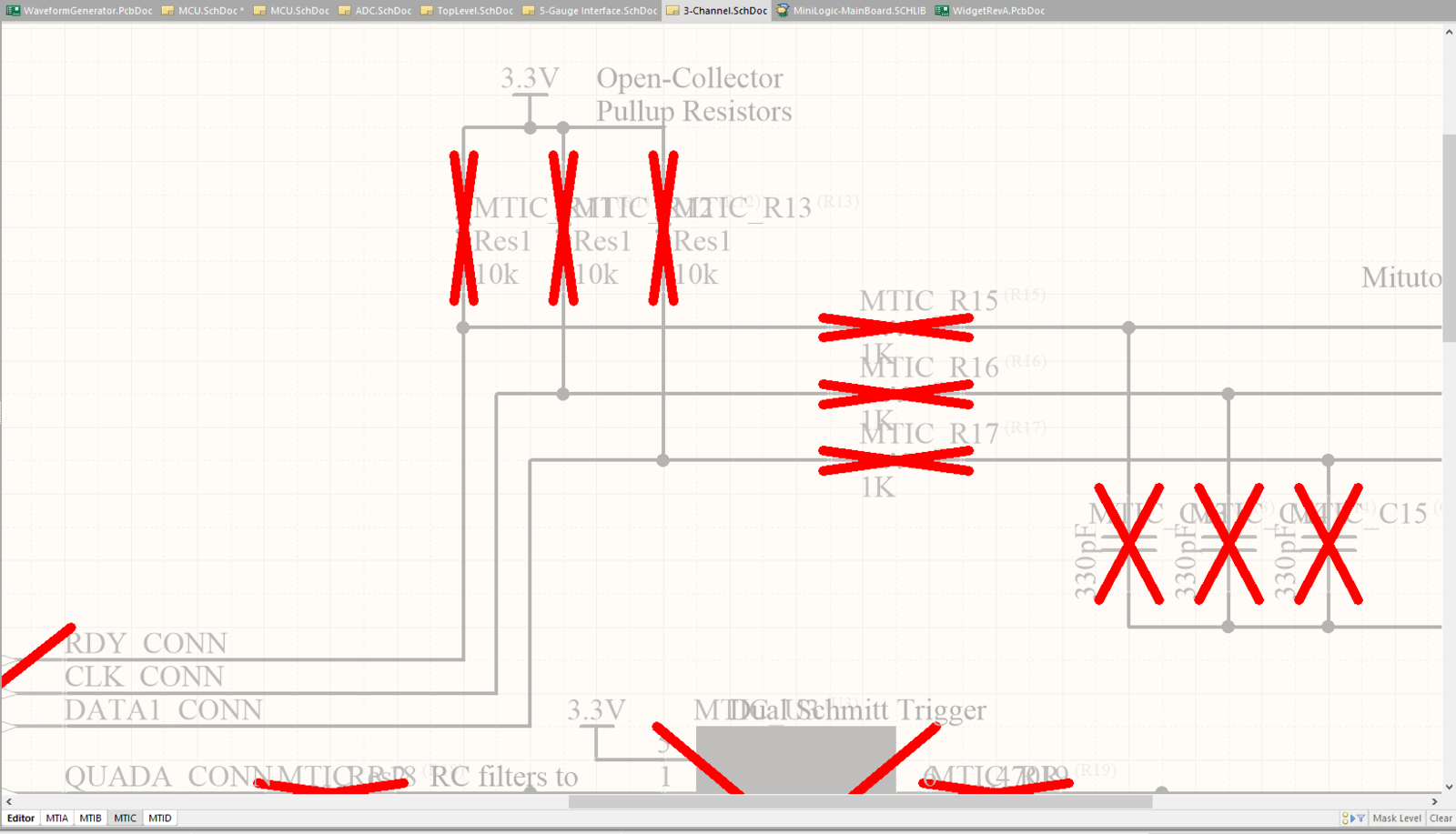
Nice! I would encourage you to double-check all sheets of your schematic when creating design variants, as this is an easy way to spot mistakes (such as a component that has been marked Not Fitted by accident).
Generating Outputs - BOM
Now comes the most powerful part of creating design variants - generating design outputs! The first document we'll generate is the Bill of Materials, or BOM. The BOM lists all of the manufacturer part numbers in your design and links each one to a schematic component. This document is very important to the PCB assembly house, who typically purchases the components in the BOM and loads them into a pick-and-place machine.
When managing design variants manually, it's necessary to indicate which components and designators will not be populated. One way to do this is to label the unused components with DNI (Do Not Install), DNP (Do Not Populate), Not Fitted, or something similar. Unsurprisingly, this is not a fool-proof solution, as some manufacturers may not recognize or understand these directives.
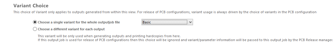
A better way is to eliminate the unused components and designators from the BOM entirely. Sure, you can delete them by hand, but this is inherently error-prone and can be quite time-consuming. Instead, let's let Altium handle this for us. In your Output Job file (if this is a new project, you may have to add one using File -> Add New to Project -> Output Job File), select the appropriate design variant from the top of the window:
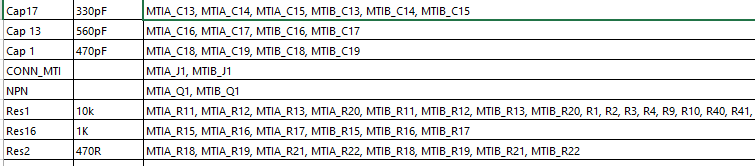
Then, simply generate your BOM. I selected the basic version of my PCB, which omits two of the four device channels. Let's see what happened. The first image below is the default BOM, which does not omit any channels. Notice that you can see components with MTIA, MTIB, MTIC, and MTID prefixes.

The second image shows the BOM generated for the Basic variant, which shows only MTIA and MTIB components.
Nice!
Generating Outputs - Pick-and-Place
The second document of importance is the Pick-and-Place file, which contains the location and orientation of each component in the assembly. This is the file used by pick-and-place machines to mount components on a PCB prior to soldering.
Components that are not populated on the PCB are almost always marked as such on the BOM (or removed entirely as discussed above). The pick-and-place file is often neglected, which sometimes leads to confusion during the assembly process. I have seen situations where the "DNP" designator on the BOM was missed, and DNP components were installed anyway. Had those parts' entries on the pick-and-place files been omitted as well, the assembly house would not have loaded the components in the pick-and-place machine in the first place.
Generating a pick-and-place file for your assembly variant is very simple. From the PCB Editor, make sure the proper variant is selected by choosing it from the drop-down menu on the toolbar (just as you did from the Schematic Editor earlier). Then, click File -> Assembly Outputs -> Generates Pick and Place Files. Voila!
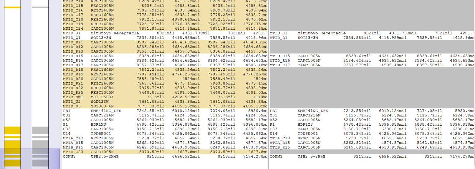
Below is a WinMerge comparison between the default and variant pick-and-place files, which clearly shows that the DNP parts are completely omitted from the variant version. Even though it's not essential to generate the pick-and-place file this way, it's an additional way to validate the design during the hand-off to the manufacturer.
Summary
Design Variants in Altium are a powerful tool for handling situations where a base design can be assembled into multiple versions or "flavors." This article covered the case where parts are not populated to create a "Basic" version (where the base design is the "Deluxe" version with more functionality). Design Variants can be used to change part parameters (like a resistor value or a part number) as well. If you find yourself managing a lot of design outputs manually, it might be time to let Altium shoulder the brunt of the work for you!
Learn more about DMC's embedded design and circuit design services.