Recently, I’ve needed to do some proof of concept testing for a LabVIEW-based project. The only special I/O requirement for my prototype was a +/- 10V analog output that is capable of sourcing at least 1mA of current. The good news was that DMC owned just the piece of hardware: an NI USB-6351 X-Series DAQ. The bad news was that it was handed to me with the caveat that it doesn’t turn on and may or may not smell bad when plugged in. Undeterred, I resolved to resurrect our $1500 out-of-warranty brick.
Since the unit showed no signs of powering on, the first order of business was to verify the main power source. Finding nothing wrong with the 12V external power adapter, I set off to get my hands dirty and investigate the internal circuitry.
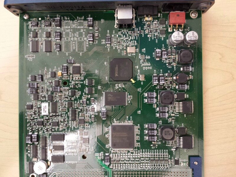
Thankfully, NI made the DAQ very easy to disassemble. The entire PCB assembly slides out in one piece after the removal of a couple screws. Nothing seemed charred or obviously damaged and nothing dramatic happened when I tried giving it power again. So, I started the highly technical operation of poking around at various chips to see if anything was hot.
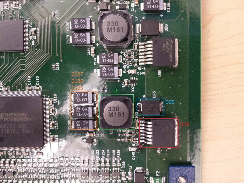
Nothing felt scalding hot, but there was a section of circuitry warm enough to raise suspicion. Especially so because a nearly identical set of components nearby was cool to the touch. The hot circuits included an LM2673-ADJ adjustable switching regulator (U54) connected to a 33uH power inductor (L6) and 5A-rated BAT540C Schottky diode (D25). The circuit was regulating the 12V from the external adapter to a somewhat strange 1.2V. The neighboring circuit, on the other hand, was taking the same 12 volts and outputting a standard 3.3V.
Checking the datasheet for the LM2673-ADJ, I discovered that its output voltage is controlled by a resistive voltage divider. I found the appropriate resistors in the PCB, measured their resistances, and calculated the designed output voltages for the two regulator circuits. The circuit supplying 3.3V was designed as such while the one outputting 1.2V should have been outputting 5V.
The most likely cause of this discrepancy was that the regulator was supplying excessive current due to a damaged component somewhere on the 5V power rail. In doing so, it would trigger its over-current and/or over-temperature protection and reduce its output voltage. I checked and found that there was indeed a very low amount of resistance between the 5V power rail and ground. Whatever component was causing this would be sinking a lot of current and therefore necessarily be quite hot.
It didn’t seem like the sort of thing that’d be hard to find.
My prime suspect was diode D25 that sits across the regulator’s 5V output and ground. I removed it only to find that 5V and ground were still shorted together. I verified with my multimeter that the diode was damaged and contributing to the short, but it clearly wasn’t the only offending component. Thinking that the problem was isolated to the immediate vicinity of the regulator, I removed output capacitors C125, C126, and C127. No dice. A little desperate, I removed the regulator chip itself.
Using an adjustable current limit lab power supply, I can feed power directly into the shorted 5V power rail. Whatever component was causing the short would surely heat up enough for me to detect. With the power supply voltage limited to 5V, I started cranking up the current. Eventually, I found myself pouring over 3A into the circuit board at a mere 1V.
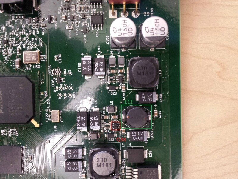
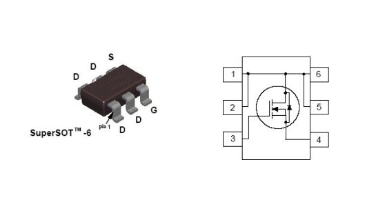
I found two potential culprits. Just above the 3.3V regulator circuit, there was a circuit block that contained a power inductor designated L11 and a tiny 6-pin surface mount component designated Q38. Both were intensely hot. Under the assumption that inductors don’t just go off and fail, I turned my attention to Q38. I could make out the markings “A41AC” yet no amount of searching yielded any useful results. Frustrated, I decided to remove the chip altogether.
As soon as Q38 was gone, the short-circuit I was hunting went with it! I knew the DAQ wasn’t fixed, but I couldn’t stop myself from attempting to power it on right there. All I had to do was plug in the external 12V power brick while simultaneously using the lab power supply to replace the 5V regulator I removed.
Once connected over USB, NI MAX detected the DAQ immediately. I was ecstatic. It amazed me that the device seemed to be functioning normally. The digital I/O seemed to work, so I went to test what I needed from the DAQ in the first place: analog output. The behavior I saw was puzzling. When commanded to output +10V, I would get +2.5V. Similarly, commanding -10V would result in -2.5V and the voltages in between scaled linearly.
Of course, the one feature I needed from this DAQ was the one that was still broken.
When additional searching turned up nothing useful regarding the mystery chip, I started reverse engineering the schematic for the circuit block in which it lived. Very fortunately for me, just like the 5V and 3.3V regulators from before, there was a doppelganger to this circuit block as well. It too contained an A41AC mystery chip. Here is the partial schematic I came up with:
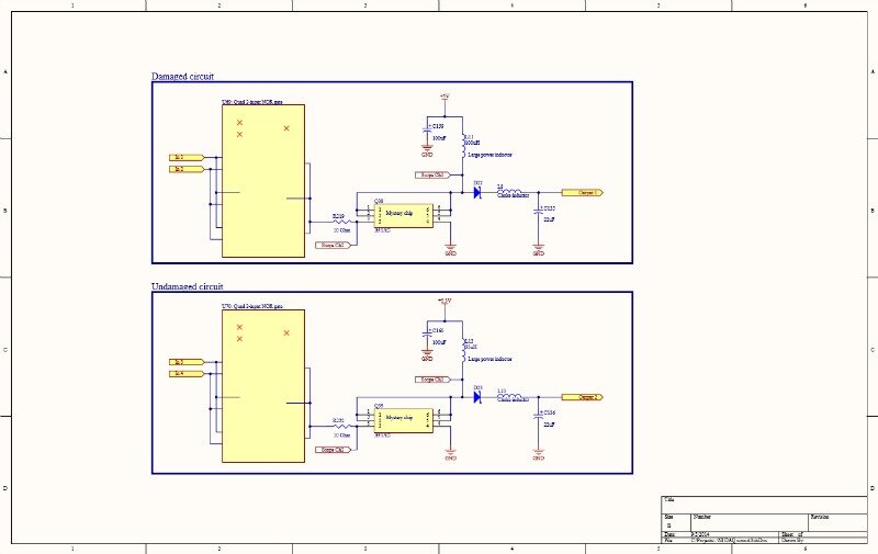
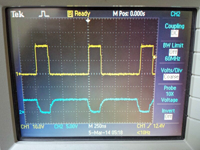
Q38 and L11 were the components that I had felt getting very hot. Q39 and L13 were cool to the touch. These two circuits look like classic voltage boost converters. To get a better feel for how these circuits worked, I used an oscilloscope to probe the undamaged circuit at the points indicated on the schematic.
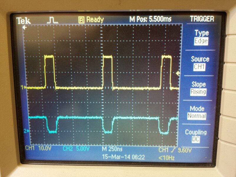
Let’s assume the mystery chips Q38/39 are N-channel enhancement mode MOSFETs. Pins 1, 2, 5, and 6 would be the drain, pin 3 would be the gate, and pin 4 would be the source. On the undamaged circuit, the scope shows a ~1MHz square wave with ~80% duty cycle at the gate. When the gate is high, the transistor turns on and pulls the drain to ground. This forces current to increase in L11, allowing it to store energy. When the gate is low, the transistor turns off, forcing the current stored in the inductor to flow through the flyback diode, D23, to the output of the circuit. This operation matches exactly that of a boost converter operating in continuous mode.
The relevant equation to be aware of here is Duty cycle = 1 – Vin/Vout. Since Vin is 3.3V and Vout is 20V, the duty cycle should be 83.5%. This result matches closely to what I saw being fed to the MOSFET gate. Out of curiosity, I checked what kind of waveform was being fed to the damaged circuit and found a ~1MHz square wave with ~75% duty cycle. With Vin being 5V in that circuit, Vout is predicted to also be 20V. At this point I speculated that the undamaged circuit was used to supply the reference for the DAQ’s +/-10V analog input and the damaged circuit supplies the reference for the analog output. With Q38 removed, the broken boost circuit would simply output the 5V that it was fed. This explains why I could only get the DAQ’s analog output to swing between -2.5V and +2.5V.
Now it’s time to tackle the issue of actually finding a replacement part for Q38. Using calipers, I measured the dimensions of the chip to match the TSOT-23-6 package. Searching for N-channel MOSFETS in this package on DigiKey, I found several pin-compatible parts!
Extremely satisfied with myself, I ordered a FDC5661N_F085 which had the highest rated power rating at 1.6W. I also grabbed a BAT540C and LM2673-ADJ to repair the 5V regulator circuit before running around the office to gloat over my victory.
The parts came in the mail the next morning and I eagerly got to work soldering them in their places. I first restored the 5V regulator circuit which fired up without a hitch. After that I dropped a new MOSFET to replace Q38. Giving myself a pat on the back, I powered up the DAQ to run a final test. This time, none of the DAQ’s status LEDs showed any activity. Not five seconds later, I detected a burning smell and saw the dreaded trail of smoke emanating from the new MOSFET.
After cutting the power and staring at the circuit board for a while in bewilderment, I set off to find out what went wrong. I made sure that I installed the MOSFET in the correct orientation and verified that its drain and source were not shorted together. The fact that the new MOSFET was burning up so quickly and taking out the entire power rail with it could mean that electrically it was connected directly across +5V and ground.
I decided it wouldn’t hurt too much to try to see what was going on with the oscilloscope. I hooked it up to the new MOSFET just as I had done previously with the undamaged circuit. I was able to get this trace by briefly toggling power to the board:
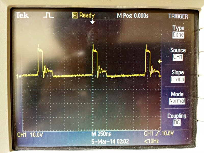
The strange waveform didn’t reveal much more information than I already knew. At least it was interesting to see the electrical havoc being wreaked.
I checked diode D22 to make sure nothing on the output side of the circuit could interfere with the MOSFET. That leaves us with a single remaining suspect: power inductor L11. Since inductors are simply coils of wire, I was incredulous that it could be damaged. Furthermore, a resistance measurement will reveal that they are indistinguishable from a simple wire.
Lacking an inductance meter, I set about building an inductor test circuit. Inductors resist changes to the current flowing in them, as shown by their characteristic equation: V = L * (di/dt). Applying a voltage V across the inductor will cause current to rise linearly with a slope of (V/L). The test setup I made looked like this:
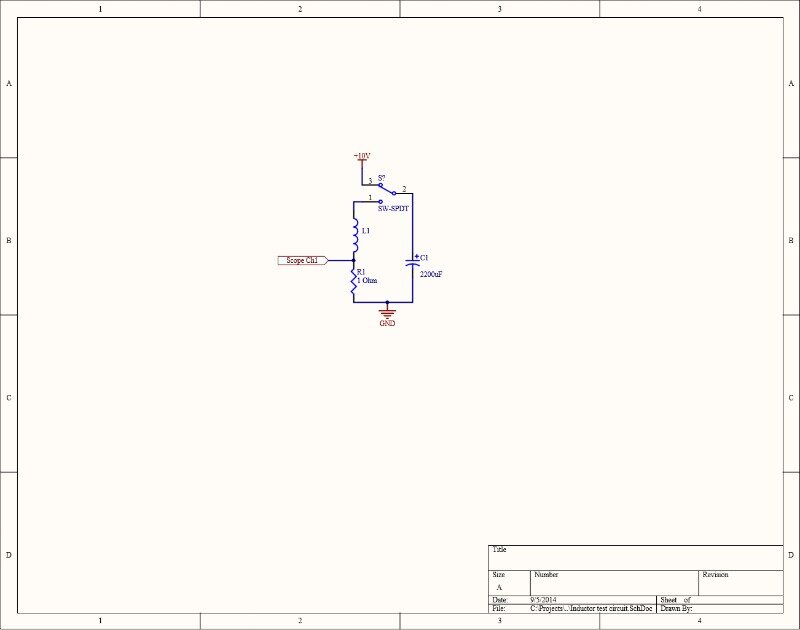
The inductor under test was connected in series with a 1 ohm resistor. The oscilloscope measured the voltage across the resistor which would indicate how much current was flowing at any given time. The capacitor would be charged to 10V before being discharged through the inductor. Its purpose was to provide a low-impedance voltage source to the inductor under test.
First, I ran my test using a known good 33uH inductor I found in the lab. Here is what the scope trace looked like:
The current initially rose linearly for about 10us before jumping up to 10V. The discontinuity happened due to the core of the inductor reaching saturation. The slope of the linear region was slightly under 0.4V/us (which corresponds to 0.4A/us). Since V = 10V, we’d shown, experimentally, that the inductor was around 25-30uH.
I removed L11 from the circuit board and ran the same test. Here is the scope trace:
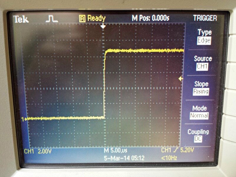
This time, the current jumped up to 10A immediately, showing that the inductor was behaving as a short. When this inductor shorted for an unknown reason, it caused a huge current to flow through Q38 whenever it was switched on. I figured that the 5V regulator would go into current limiting mode, dipping its output voltage to the 1.2V I measured at the beginning of my investigation. After several red herrings, we’d finally found the actual culprit!
The only thing left to do was to find a suitable replacement inductor. I found and ordered a 100uH inductor (Bourns PM3316-101M-RC) that had an almost identical footprint to our shorted inductor. In the meantime, I was impatient to get the DAQ working again. Referring back to the Wikipedia page on boost converters, we could see that as long as they were operating in continuous mode, the output voltage depended only on the switching duty cycle and was completely independent of inductance.
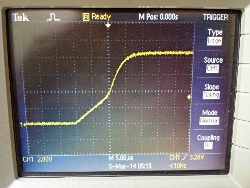
Feeling adventurous, I shoehorned the 33uH power inductor I found lying around into the circuit. I also replaced Q38 with another fresh MOSFET. With the oscilloscope connected, I cautiously turned on the power. Just like that, the DAQ came to life without any drama. I measured a solid 20V output from the repaired boost converter circuit and the scope trace showed a clean waveform:
I connected the USB DAQ to my computer and was able to get accurate and precise analog voltage outputs across the entire +/-10V range. Exhausted and relieved, I finally started on the proof-of-concept project for which I need the NI USB-6351 in the first place.
Learn more about DMC's LabVIEW programming services.