In this section, we'll discuss data acquisition using the multiple FPGA chassis architecture outlined in the previous section, NI LabVIEW Part 1: Building Distributed and Synchronized FPGA Applications with Multiple C Series Chassis. If you haven’t already, refer to Part 1 of 3 for Distributed FPGA Chassis Time synchronization.
We use LabVIEW DMA FIFOs for typical FPGA applications that acquire data to be sent to an RT target(Host). There are a lot of ways to use FIFOs for transporting data from the FPGA to the RT target. We will outline several of these options and present a generalized data transfer mechanism for synchronized DAQ on multiple chassis.
Let's start by outlining our requirements and then build then up a solution which considers several different options for transferring data from the FPGA to the host.
Outlining the Requirements
Requirements:
- The system has a high channel count.
- There are a variety of different data types in the channels being acquired.
- Channels may be acquired from different loops that execute at different loop rates.
- Channel data acquisition times must be synchronized across multiple chasses.
Schemes for Transferring Data
The DMA FIFO is the fundamental block for lossless transfer of data between an FPGA application and the host.
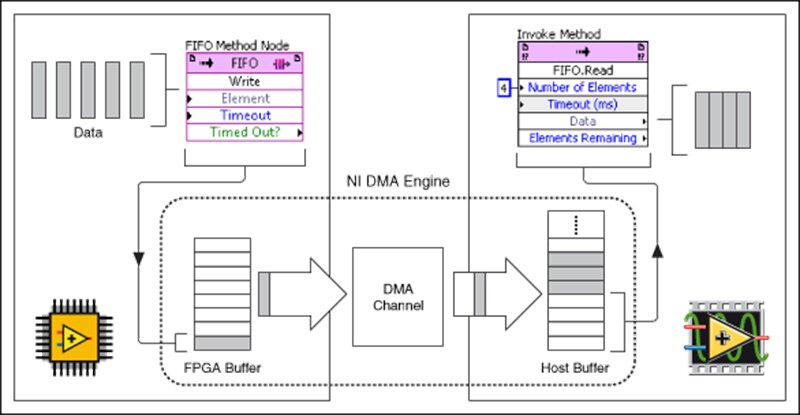
Using this building block, let’s discuss the progression of a generalized DAQ architecture starting with a single chassis implementation.
Single Channel Data Transfer
The simplest scheme for transferring channel data is when you’re acquiring data for a single channel.
In this scenario, you can write the data into the FIFO as it’s being acquired. As the host is acquiring data from the FPGA, it is guaranteed to be a sequential, ordered series of samples for that channel.
Multi-Channel Data Transfer
In most instances, we will want to acquire more than (1) channel of data, so the natural next step for this is to interleave the data that is being written to the FIFO. For a fixed channel list, this interleaved ordering can be pre-defined. That data can then be decimated using that ordering when it is read from the host.
Example FIFO ordering:
[channel 1 – sample 1, channel 2-sample 1, ch3-s1, … , chN-s1],
[channel 1 – sample 2, channel 2-sample 2, ch3-s2, … , chN-s2],
… ,
[channel 1-sample N, channel 2-sample N, ch3-sN, …, chN-sN]
Differing Acquisition Rates
In the most generalized approach, it is not guaranteed that every channel will be acquired at the same rate. If you only have a few different acquisition rates, you could potentially use a separate FPGA-to-Host FIFO for each acquisition loop/rate.
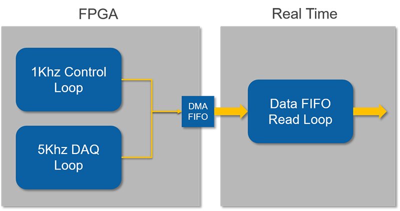
If you can only use a single FIFO for transferring data or have more DAQ loop rates than FIFO channels, we would like to be able to use a single FIFO for acquiring data from all of the different sources/loops in our application.
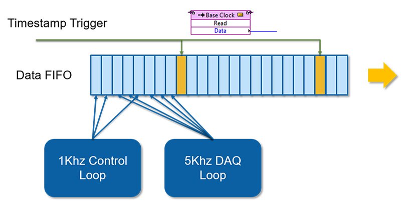
In the example shown below, we have a 1Khz control loop that may contain some output channels or internal calculated channels that we would like to acquire as well as a more standard DAQ loop running at 5Khz.
Including Additional Information
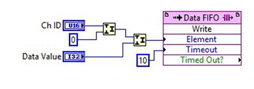
We can no longer assume what the ordering of the channels written to the FIFO will be, so we need to include additional information along with each channel’s sample value to identify it on the Host. By setting the FIFO data type to be u64, we can pack additional information to be included with each channel.
In the example below, we can include a channel ID in addition to the channel data’s value so the Host can parse which value is associated with which channel ID.
What About Timing?
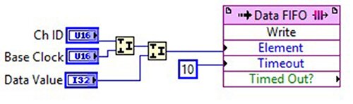
With the single channel acquisition or interleaved approach, we can infer the time delta between each sample. When capturing channels throughout a general FPGA application, we should have a strategy for capturing timing information with the samples we’re acquiring. One way to achieve this is to include a base clock value that is packed along with the channel ID and channel value:
Another option, if your application can tolerate less resolution per channel, would be to periodically send a special timestamp channel value at a regular interval. This unique timing channel can be used on the host side for determining when to aggregate a set of channel data. It can attach a single timestamp to all of the channel values received since the last timestamp value was received through the FIFO.
Considering Scale
The final step for this architecture is to consider how it scales with multiple FPGA chassis. In the previous section, we were able to generate a synchronized base clock value across all chassis. By using this synchronized base clock as the time stamp included with the channel values, we can achieve synchronized data acquisition across multiple chassis.
In the diagram below, you can see what this architecture might look like on the RT/Host side. Multiple parallel loops will be used for acquiring data from the FIFOs, Scaling the data, and then aggregating the data to be disseminated throughout the RT-Host application.
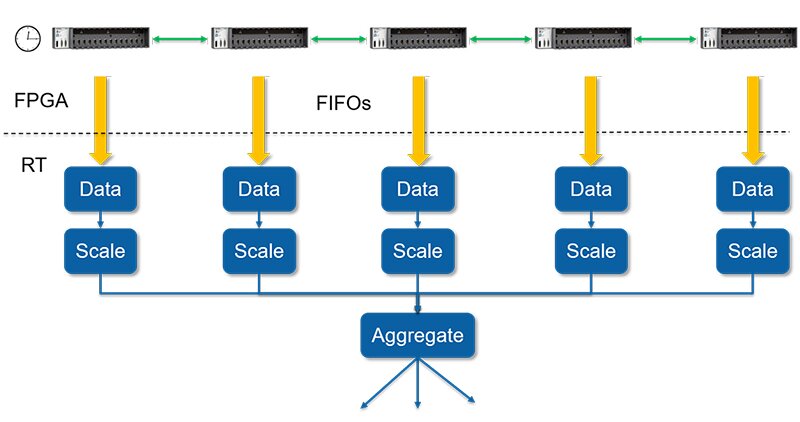
The last part of the architecture considers how to share data between chassis without involving the RT.
Stay tuned for synchronous data sharing between FPGA chassis using NI 9853 CAN module!
Learn more about DMC's FPGA programming expertise.